 Categories
 Brands
 Information
 Shopping Cart
 Bestsellers


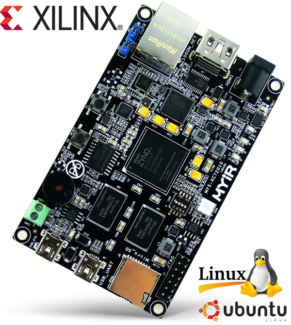
Z-turn Xilinx Zynq-7020 board - MYS-7Z020-C-S
 Click to enlarge |
|
Z-turn Board |
|
|
Overview
The Z-turn Board is a low-cost and high-performance Single Board Computer (SBC) built around the Xilinx Zynq-7010 (XC7Z010-1CLG400C) or Zynq-7020 (XC7Z020-1CLG400C) All Programmable System-on-Chip (SoC) which is among the Xilinx Zynq-7000family, featuring integrated dual-core ARM Cortex-A9 processor with Xilinx 7-series Field Programmable Gate Array (FPGA) logic.
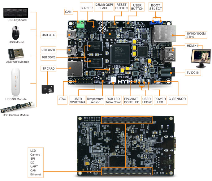
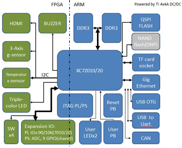
The Z-turn Board takes full features of the Zynq-7010 / 7020 SoC, it has 1GB DDR3 SDRAM and 16MB QSPI Flash on board and a set of rich peripherals including USB-to-UART, Mini USB OTG, 10/100/1000Mbps Ethernet, CAN, HDMI, TF, JTAG, Buzzer, G-sensor and Temperature sensor. On the rear of the board, there are two 1.27mm pitch 80-pin SMT female connectors to allow the availability of 96 / 106 user I/O and configurable as up to 39 LVDS pairs I/O.
The Z-turn Board is capable of running Linux operating system. MYIR has provided Linux 3.15.0 SDK, the kernel and many drivers are in source code. The board is delivered with complete accessory kit including two USB cables, one Ethernet cable, one HDMI cable, one 4GB TF card and one 5V power adapter and product CD-ROM which enables you to start the development quickly when getting the board out-of-the-box. MYIR also offers optional WiFi and camera modules, Z-turn IO Cape for the Z-turn Board. The Z-turn IO Cape provides many peripheral signals and interfaces including ADC, GPIO, LCD, Camera and three Pmod interfaces.
The Z-turn Board is an excellent development platform for evaluating and prototyping for Zynq-7000 SoC. It can also be used as a System-on-Module (SOM) for your next embedded design; typical applications are Industrial Automation, Test & measurement, Medical Equipment, Intelligent Video Surveillance, Aerospace and military, etc.
Features
Item
Features
SoC
Xilinx XC7Z010-1CLG400C (Zynq-7010) or XC7Z020-1CLG400C (Zynq-7020)
- 667MHz ARM® dual-core Cortex™-A9 MPCore processor (up to 866MHz)
- Integrated Artix-7 class FPGA subsystem
with 28K logic cells, 17,600 LUTs, 80 DSP slices (for XC7Z010)
with 85K logic cells, 53,200 LUTs, 220 DSP slices (for XC7Z020)
- NEON™ & Single / Double Precision Floating Point for each processor
- Supports a Variety of Static and Dynamic Memory Interfaces
Memory
1GB DDR3 SDRAM (2 x 512MB, 32-bit)
Storage
16MB QSPI Flash
TF card interface
Communications
1 x 10/100/1000M Ethernet
1 x CAN
1 x Mini USB2.0 OTG
1 x USB-UART debug interface
Display
1 x HDMI (supports 1080p resolution)
We are using evaluation version of Xylon's logiCVC-ML and logiCLK IP core.
Please contact Xylon to buy the license of the IP core for logiCVC-ML or logiCLK.
http://www.logicbricks.com/Products/logiCVC-ML.aspx
http://www.logicbricks.com/Products/logiCLK.aspx
User I/O
Brought out via two 1.27mm pitch 80-pin SMT female connectors
- 90/106 user I/O (7010/7020)
- Configurable as up to 39 LVDS pairs I/O
Dimensions
63mm x 102mm x 1.6mm (8-layer PCB design)
Power supply
USB power supply or DC 5V/2A
Others
Onboard three-axis acceleration sensor and temperature sensor
1 x 2.54mm pitch 14-pin JTAG interface
2 x Buttons (1x Reset, 1 x User)
4-channel toggle switch
5 x LEDs (3 x User LEDs, 1 x Power indicator, 1 RGB LED)
1 x Buzzer
OS support Linux 3.15.0
Target Applications
Evaluation and Prototyping for Zynq-7000 AP SoC
Industrial Automation
Test & measurement
Medical Equipment
Intelligent Video Surveillance
Aerospace and military
Hardware Features
The Zynq™-7000 family of devices combines the software programmability of a Processor with the hardware programmability of an FPGA, resulting in unrivaled levels of system performance, flexibility, scalability while providing system benefits in terms of power reduction, lower cost with fast time to market. Unlike traditional SoC processing solutions, the flexible programmable logic of the Zynq-7000 devices enables optimization and differentiation, allowing designers to add peripherals and accelerators to adapt to a broad base of applications.
The Zynq-7000 AP SoC leverages the 28nm scalable optimized programmable logic used in Xilinx’s 7 series FPGAs. Each device is designed to meet unique requirements across many use cases and applications. The Z-7010, Z-7015, and Z-7020 leverage theArtix®-7 FPGA programmable logic and offer lower power and lower cost for high-volume applications. The Z-7030, Z-7035, Z-7045, and Z-7100 are based on the Kintex®-7 FPGA programmable logic for higher-end applications that require higher performance and high I/O throughput.
|
Z-7010 |
Z-7015 |
Z-7020 |
Z-7030 |
Z-7035 |
Z-7045 |
Z-7100 |
|
|
Processor Core |
Dual ARM® Cortex™-A9 MPCore™ with CoreSight™ |
||||||
|
Processor Extensions |
NEON™ & Single / Double Precision Floating Point for each processor |
||||||
|
L1 Cache |
32 KB Instruction, 32 KB Data per processor |
||||||
|
L2 Cache |
512 KB |
||||||
|
On-Chip Memory |
256 KB |
||||||
|
Memory Interfaces |
DDR3, DDR3L, DDR2, LPDDR2, 2x Quad-SPI, NAND, NOR |
||||||
|
Peripherals |
2x USB 2.0 (OTG), 2x Tri-mode Gigabit Ethernet, 2x SD/SDIO |
||||||
|
Logic Cells |
28K Logic Cells |
74K Logic Cells |
85K Logic Cells |
125K Logic Cells |
275K Logic Cells |
350K Logic Cells |
444K Logic Cells |
|
BlockRAM (Mb) |
240 KB |
380 KB |
560 KB |
1,060 KB |
2,000 KB |
2,180 KB |
3,020 KB |
|
DSP Slices |
80 |
160 |
220 |
400 |
900 |
900 |
2,020 |
|
Transceiver Count |
4 (6.25 Gb/s) |
up to 4 (12.5 Gb/s) |
up to 16 (12.5 Gb/s) |
up to 16 (12.5 Gb/s) |
up to 16 (10.3125 Gb/s) |
||
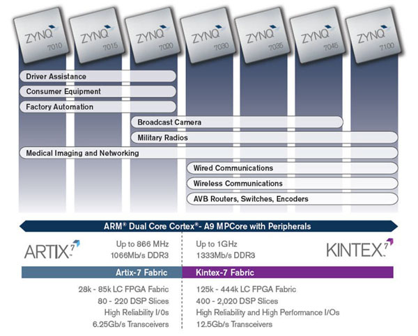
Zynq-7000 Devices
Z-turn Board Function Block Diagram
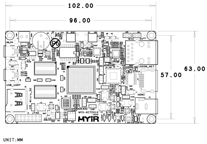
Z-turn Board Dimension Chart
|
<
|
Your Review: Note: HTML is not translated!
Rating: Bad Good
Enter the code in the box below:

Click to enlarge

Click to enlarge
 Z-turn IO Cape - MY-CAPE001 MY-CAPE001 $40.00 |